Honey-like heat flow: A new heat transport regime discovered in ultrathin semiconductors

Controlling heat flow is a major challenge for many technologies. In electronic and photonic devices, for example, heat dissipation can limit the performance and efficiency, as well as their potential for further miniaturisation. At the same time, two-dimensional (2D) materials, which are made of layers just a few atoms thick, have emerged as a promising platform in these fields. For example, 2D semiconductors are expected to be used in conduction channels of future transistors. However, their thermal behaviour remains difficult to predict and control.

Now, an international team of researchers led by ICN2, UAB, TU/e, and McGill has discovered a new regime of heat transport in ultrathin materials. The study shows that in 2D semiconductors, in particular molybdenum disulfide (MoS₂) and molybdenum diselenide (MoSe₂), heat can behave in a completely new way, known as hydro-thermoelastic transport, where thermal diffusion is highly impeded. These findings, published in Nature Physics, could have a significant impact on the development of new strategies for thermal management in devices.

A combination of unexpected phenomena

Under normal conditions, heat spreads gradually from hot regions to cold ones. However, in these ultrathin materials, more complex effects occur. As Dr Sebin Varghese, first author of the paper, remarks: “Our results challenge the conventional picture of diffusive heat transport and reveal a richer, more complex transport mechanism in ultrathin semiconductors.” One of the effects that occur is phonon hydrodynamics, whereby heat is carried collectively and behaves like a viscous fluid. At the same time, heating induces mechanical deformations in the material, which also affect how heat moves. Although these types of effects were already known, they had never been observed in this type of materials.

The interplay of these phenomena results in unexpected behaviour: heat propagates much more slowly than predicted, with the thermal diffusivity reduced by up to an order of magnitude. To reach these conclusions, the researchers used an advanced optothermal technique that enabled them to track heat flow in real time with nanometre resolution. Prof. F. Xavier Alvarez from the Department of Physics at the UAB, who led the theoretical part of the work, notes that “for the first time, we observe how mechanical stress can redirect — and even obstruct — the flow of heat in a material.”

Can heat flow “the opposite way”?

The experiments show that, in these ultrathin materials, heat tends to remain concentrated around the heated region for longer than expected. This happens because heating causes the material deformations that alter how heat moves through the material, even pushing the heat flow in unexpected directions.

As Prof. Klaas-Jan Tielrooij (ICN2 and TU/e), who led the study, explains: “What surprised us most is that heat can, under certain conditions, resist leaving the hot region, which is due to contributions to the heat flux that point from cold to hot regions, rather than the conventional flux that points from hot to cold regions. This opens up a completely new way to control heat flow intrinsically, without the need to modify the material’s structure.”

This discovery provides new fundamental insight into how heat is transported at the nanoscale and could pave the way for designing electronic, photonic, and thermal devices with new functionalities. The ability to control rather than simply dissipate heat could be pivotal for future technologies, from improving the thermal management of chips to making thermoelectric systems more efficient.


Also Read:

More power extraction from solar cells found

How mineral-rich Japan can dictate world now?

US Semiconductor Tariffs: India Faces Limited Immediate Impact

The U.S. decision to impose tariffs on semiconductors is unlikely to significantly impact India in the short term, as the country is not a major chip exporter to the U.S., industry experts said Thursday.

With India already imposing zero import duties on semiconductors, the country faces no immediate trade retaliation concerns, said Ashok Chandak, president of the India Electronics and Semiconductor Association (IESA).

Most of India’s upcoming semiconductor manufacturing and assembly facilities cater to global brands, and its growing domestic demand will be met primarily through local production.

In the long run, Indian chipmakers are expected to remain competitive, as the U.S. tariff applies uniformly to all exporting nations, Chandak noted.

The Trump administration’s decision to impose tariffs of 25% or more is expected to reshape the global semiconductor industry, affecting costs, supply chains, and innovation.

The new tariffs will significantly increase the cost of chips imported into the U.S., particularly from dominant manufacturing hubs like Taiwan, South Korea, and China. These additional costs will likely be passed on to consumers, driving up prices for smartphones, laptops, electric vehicles, and industrial electronics.

Tech giants such as Apple, NVIDIA, and Tesla could see rising production costs, potentially squeezing profit margins or forcing them to raise consumer prices, according to IESA.

To mitigate risks, companies may explore alternative supply chains or invest more in domestic chip production. However, semiconductor fabrication plants are among the most capital-intensive projects, requiring $10 billion to $25 billion per site.

“Companies must weigh multiple factors before making investment decisions, including workforce availability, tax policies, regulatory frameworks, and environmental considerations,” IESA stated.

Using chirality for faster, smaller, and more efficient data storage devices

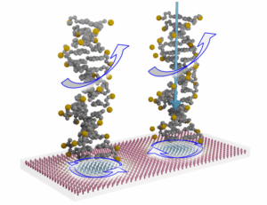
Researchers at Johannes Gutenberg University Mainz (JGU) are pursuing a completely new and unconventional strategy to improve the way data can be processed and – in particular – stored. The team members, based in Mainz and Jerusalem, have come up with the idea of bringing together two different forms of chirality to develop new data storage systems that are faster, smaller, and more efficient than those currently available.

Chirality, also known as handedness in this context, describes objects that come in two distinctly different configurations that are mirror images of each other such as our left and right hand. “We were inspired by nature, where chirality is a common phenomenon. Chiral molecules can act like a filter for electron spin and ensure functionality even on the smallest scale,” said Professor Angela Wittmann of the JGU Institute of Physics.

Combining the chirality of spin configurations and molecules

In their approach, the researchers from the fields of experimental solid state physics, atomic physics, and molecular chemistry will be using recently discovered chiral spin structures. These so-called skyrmions are tiny vortices in magnetic thin films protected by their chirality. It is this kind of chiral magnetic texture that the researchers intend to combine with chiral molecules over the course of the project. The assumption is that, based on the chiral-chiral interaction, they would have a unique, flexible, controllable, and efficient means of manipulating spin structures. “With the help of a chiral molecule, it should be possible to switch the handedness of the chiral magnetic textures in thin films, for instance, from clockwise to anticlockwise,” clarified Wittmann.


Two chiral molecules on chiral spin structures in a magnetic thin film/Two chiral molecules on chiral spin structures in a magnetic thin film (ill./©: Angela Wittmann)

In this case, the chiral molecule with its DNA-like helix structure would act like a spin filter, allowing only certain electrons moving in one direction to pass while holding others back. The researchers will use highly sophisticated sensor technologies to determine how and whether this interaction actually works.

“Our project is groundbreaking in that it brings together two different types of chirality,” emphasized Wittmann. According to the researchers, there is a very real chance that their innovative concept involving the utilization of spintronic components will result in the creation of the next generation of innovative storage, logic, and sensor devices that could be employed in unconventional computing.

The consortium consists of four members of Johannes Gutenberg University Mainz and two members of the Hebrew University of Jerusalem, who will be contributing their expertise in various disciplines. At JGU, these are Professor Angela Wittmann and Professor Mathias Kläui of the Condensed Matter Physics group, Professor Dmitry Budker of the Quantum, Atomic, and Neutron Physics group and the Helmholtz Institute Mainz (HIM), and Professor Eva Rentschler of the Department of Chemistry, collaborating with their partners Professor Yossi Paltiel and Professor Nir Bar-Gill of the Department of Applied Physics at the Hebrew University of Jerusalem.

Carl Zeiss Foundation sponsoring innovative projects through its new CZS Wildcard program

In early 2022, the Carl Zeiss Foundation launched its CZS Wildcard program with the objective of promoting unconventional, interdisciplinary research in the STEM field. Each team must consist of at least three researchers. The purpose of the program is to support projects that are still in a very early phase of realization and are built on original and unconventional concepts with a high potential for innovation. The first five teams will be starting work in early 2023

Also Read:

Detecting Alzheimer’s disease in the blood using Digital ICA

Turning fish waste into quality carbon-based nanomaterial

Imagine World Map Without Humans, Here It Is!